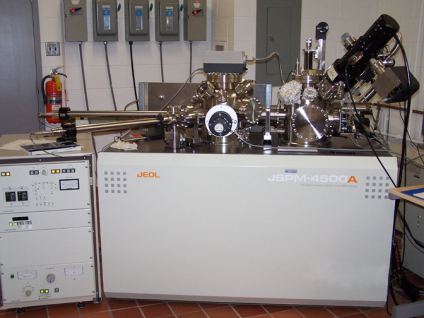
Role of the equipment
A Scanning Probe Microscope (SPM) is an apparatus able to detect the true three-dimensional topography of a given surface with nanometer resolution laterally and Angstrom resolution vertically. The surface is interacting with a sharp tip which is scanned across the sample surface. The strength of the interaction is controlled by an internal electronic circuit which also processes the signals and delivers an accurate image of the sample’s topography.
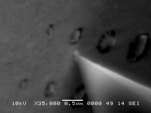
This system is designed to measure under ultrahigh vacuum and therefore can reach atomic resolution both as a Scanning Tunneling Microscope and as an Atomic Force Microscope. Surface cleaning can be performed by heating the sample in-situ either directly or indirectly. This instrument has the unique feature to be coupled with a Scanning Electron Microscope allowing to visualize/correct the location of the SPM tip on the sample in real time, and therefore to precisely position the tip at a specific location of the sample (e.g. to investigate a structure of very small dimension).
Technical specifications
• Maximum sample size: lateral: 7 mm, height: 2 mm; ideal dimensions : 7×3 mm², 0.5 mm in height (required for in situ cleaning-heating);
• Measurement location within an area 3×3 mm² around the center.
• Measurement pressure: <5×10⁻⁸ Pa.
• ~ 0.05 nm rms noise level (in Z) with turbo pump OFF.
• Maximum scanning size: X and Y: 10 µm, Z: 2 µm
• Imaging modes: true non contact (frequency feedback), intermittent contact (feedback in amplitude), contact (deflection feedback).
• Additional signals available during imaging: friction (all modes), phase and amplitude (all dynamic modes); also the current through the sample (all modes).
• Advanced techniques: electrostatic force microscopy (EFM), magnetic force microscopy (MFM), PLL loop for frequency shift detection
Accessories
• Scanning Electron Microscope for in-situ imaging the SPM measurement
• Leak system for introducing gases in the chamber, for studying the deposition/growth of molecules on a substrate of choice.
• Electromechanical characterization kit: Lock-in amplifier (Signal Recovery 7265), DC bias source (Keithley 2400).
Examples of available processes and services
• Study of the growth of nanostructures.
• Material contrast through adhesion/friction or phase of the cantilever oscillations.
• Mapping of the surface electrical resistance
|